Index
Data based modelling of the selective wave soldering process to predict solder quality (SmartSelective)
ColEP – Collaborative Usage of Data in Electronics Production
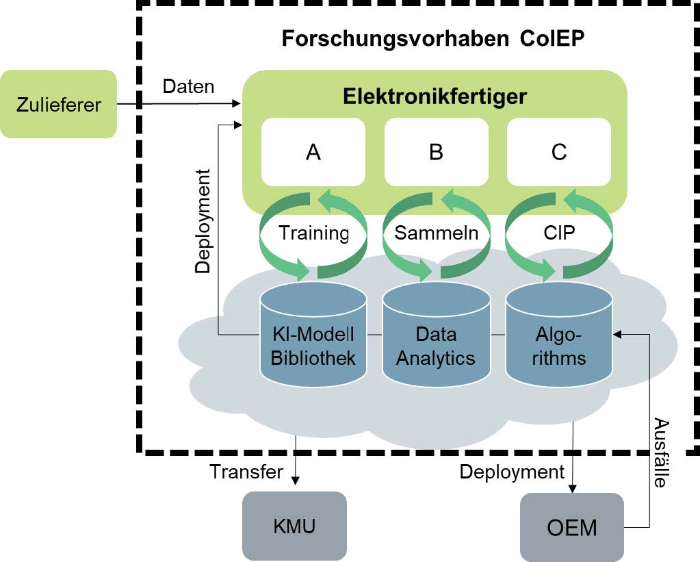
A key challenge for the use of data-based methods for the analysis and optimization of processes in electronics production is the imbalance of the data. Despite the large amounts of data generated in high-volume production, the information content of the data is limited, as the vast majority of inspections do not detect any errors. In order to avoid error slippage, the automated inspection steps, which are usually based on conventional image processing methods, are set so sensitively that there is usually a relatively high rate of pseudo errors. These components actually meet the specifications, but are incorrectly classified as faulty, resulting in a high manual inspection effort.
In order to reduce this effort, components identified as faulty can be rechecked using AI methods so that some of the pseudo faults are recognized, which results in a reduction of the testing effort. The quality of the AI methods used crucially depends on the amount and quality of the available data. In order to have a large database available despite the unbalanced data situation in electronics production, the research project ColEP is investigating the advantages and information technology solutions for the collaborative utilization of process, quality and metadata from electronics manufacturers and system manufacturers. Selected AI use cases in electronics production will be used to analyze potential improvements for which collaborative data sets appear particularly suitable. In this regard, the data is automatically anonymized and processed to ensure basic security. Furthermore, a framework will be developed using the GAIA-X concepts to ensure the sovereignty of the data for the owner.
In this context, both frameworks for federated learning and the integration into existing sovereign data infrastructures are examined. In contrast to centralized learning, where data from different sources is collected on a central server, federated learning keeps training data local to the participating companies at all times, ensuring data security and sovereignty. Model training takes place locally, after which the trained models are sent to a central server, which combines them into a global model.
The goal of the project is to investigate the applicability of federated learning in an industrial context using use cases in electronics production. It aims towards comparing the model performance of federated learning with centralized and local learning. In addition, data protection-specific advantages of federated learning will be investigated and security-relevant challenges such as data manipulation and reconstruction of training data will be critically examined and prevented using suitable methods.
IntelRadar – Intelligent radar system through a combination of additive manufacturing, hardware-integrated computer architecture and smart test routines
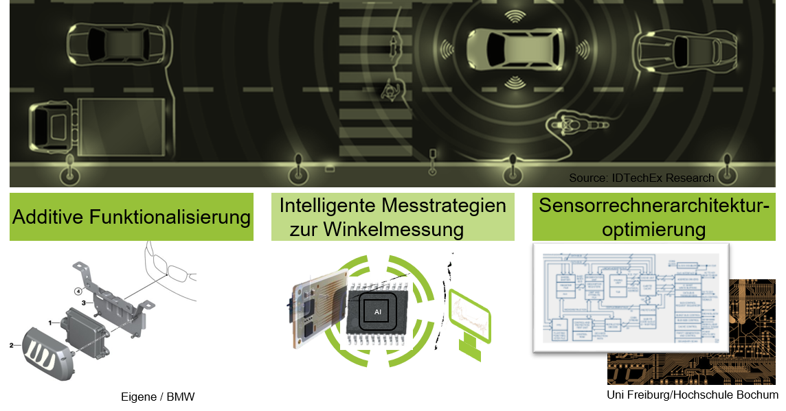
The desire for highly automated driving requires intelligent and networked vehicles that can detect their surroundings in detail and reliably using precise sensor technology. In addition to cameras, ultrasonic and lidar sensors, radar sensors are of great importance in the car of the future. Maximum accuracy and reliability, e.g. for radar-based environment detection at long distances of over 200 m, is essential. This is significantly influenced by signal scattering and attenuation, antenna quality and evaluation electronics, as well as algorithms. Due to these influences, the antenna, (secondary) radome (sensor cover) and evaluation electronics must be perfectly matched and integrated as a complete system as an essential prerequisite for precise detection. In order to minimize test and evaluation times, this also includes new approaches to functional testing through the use of artificial intelligence for sensor algorithms and sensor tests.
The aim of the project is to improve an automotive radar system along the production chain from the electronic architecture of the sensor, the development of an AI-supported test routine optimization of the angular calibration of the sensor and the integration of resistive radome heating elements by means of additive functionalization on free-form housings. This is intended to increase the reliability of the radar system. A holistic approach is being pursued, which is to be validated in the form of a demonstrator system at the end of the project.
Project goals
- Improvement of automotive radar systems
- Holistic view of the production chain
- Optimization of the radar hardware architecture
- Sensor test time reduction through AI algorithms
- Integration of resistive heating elements using printed electronics on 3D geometries
Additive Manufacture of Metal-Ceramic-Joints by means of Selective Laser Melting
Processes for additive manufacturing of 3D circuit carriers: Deriving design rules from reliability investigations
NiMm3 – Nickel-free metallization systems on 3D MID substrate materials
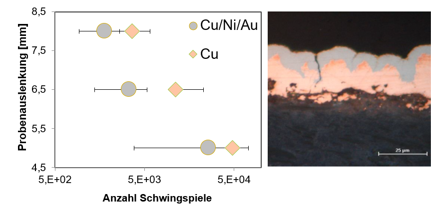
Molded interconnect devices (MIDs) are usually thermoplastic 3D substrate materials that are typically first laser direct structured (LDS) and then metallized with copper, nickel and gold without external current. In this process, the copper directly on the substrate acts as an electrical conductor, while the nickel layer provides the diffusion barrier to the gold surface. The latter enables various assembly and interconnection (AVT) techniques for electronic components, such as soldering, conductive bonding and wire bonding, to eventually obtain complex circuit carriers with a high integration density.
The reliability of metallic traces on LDS-enabled substrate materials is an essential prerequisite for the cross-breed application of MIDs. A survey of industry representatives on the subject of MID reliability revealed that delamination as well as the formation of microcracks in the conductive paths are the most common causes of MID failure. Efforts are therefore being made to eliminate these two causes as far as possible in order to significantly increase the reliability and service life of MIDs and to further promote their market penetration.
Challenge
Failure cause 1: Delamination
The choice of substrate material and the laser parameters used significantly influence both the bond strength between substrate and copper and the difference in their coefficients of thermal expansion. The latter is not only relevant for the application of MIDs at elevated temperatures, but also plays an essential role for AVT, e.g. during soldering.
Failure cause 2: microcracks
Studies within the scope of the AiF projects LDS-MID-ChaMP (16737N) and MetaZu (19754N) have shown that conductor cracks predominantly develop in the nickel layer. These microcracks expand by further loading and penetrate into the copper layer. If the load is too great, these eventually lead to failure of the conductive path and thus to failure of the circuit carrier.
Solution approach
In order to eliminate the two causes of failure mentioned above, the planned AiF project NiMm3 addresses three topics that build on each other.
1. interaction between substrate material and copper metallization
Various substrate materials are considered. In addition to thermoplastics, thermosets and ceramics are considered for an extended application range of 3D circuit carriers. By varying the laser parameter sets, the roughness and adhesion strength, and thus the reliability of the conductor track under mechanical and thermal stress (bending fatigue tests and environmental tests) are influenced. Imaging techniques such as ultrasonic microscopy (SAM) and the examination of transverse sections by scanning electron microscopy can provide further important insights.
2. alternative, nickel-free coating systems
Various nickel-free coating systems are investigated and compared with the established Cu/Ni/Au coating system. Possible variants are Cu/Ag, Cu/Sn, Cu/Pd/Au, Cu/Au and Cu/OSP (org. passivation). Here, too, conductive paths are examined under mechanical and thermal stress, among other things. Not only the layer system is varied, but also the layer thickness of the individual components.
3. AIT and influence of the soldering process
In MID technology, the assembly of electronic components is an essential step towards highly integrated circuit carriers. Therefore, the corrosion resistance and solderability or bondability of the different surface finishes are finally considered, as well as the influence of the soldering process on the adhesion strength of the metallization, e.g. by means of shear tests and SAM.
MultiPower – Customized production of highly-integrated electronic 3D power modules using multi-material vat photo-polymerisation, laser powder bed fusion and selective piezojet-metallization

The AiF-funded research project “MultiPower” aims at generating customized and highly-integrated electronic 3D power modules using various technologies of Additive Manufacturing. Multi-material photopolymerisation, laser powder-bed fusion and piezojet-printing are applied to create innovative designs with layerwise build-up. Thus, the development of suitable materials and stable processes is necessary as well as characterization and qualification of the produced interconnects. These works are accompanied and supported by simulation models.
Project advisory committee: ATN Automatisierungstechnik, Bach RC, Balver Zinn, Burms 3D Druck, Bosch Advanced Ceramics, Carbolite, GSB-Wahl, Heraeus Deutschland, Infinite-Flex, LOT-TEK, MetShape, Nanoscribe GmbH, Neotech AMT, Osram, Powerlyze, Rauschert Heinersdorf-Pressig GmbH, Rogers Germany, Schlenk AG, SEHO Systems, Sentinum, tangible engineering, Trainalytics GmbH, Vitesco, WIKA, Zollner.
ProKI-Nürnberg – Demonstration and transfer center for applying artificial intelligence in joining technology as part of the nationwide ProKI network

ProKI-Nürnberg is one of eight ProKI centers of the ProKI network in Germany. The ProKI network serves companies, especially SMEs, as a central hub for training and consultancy on using artificial intelligence (AI) in production. The focus of the ProKI center in Nuremberg lies on AI use cases in joining technology, especially in the field of electronics production and electromechanical engineering.
Further information on current events and contacts can be found on: www.proki-nuernberg.de
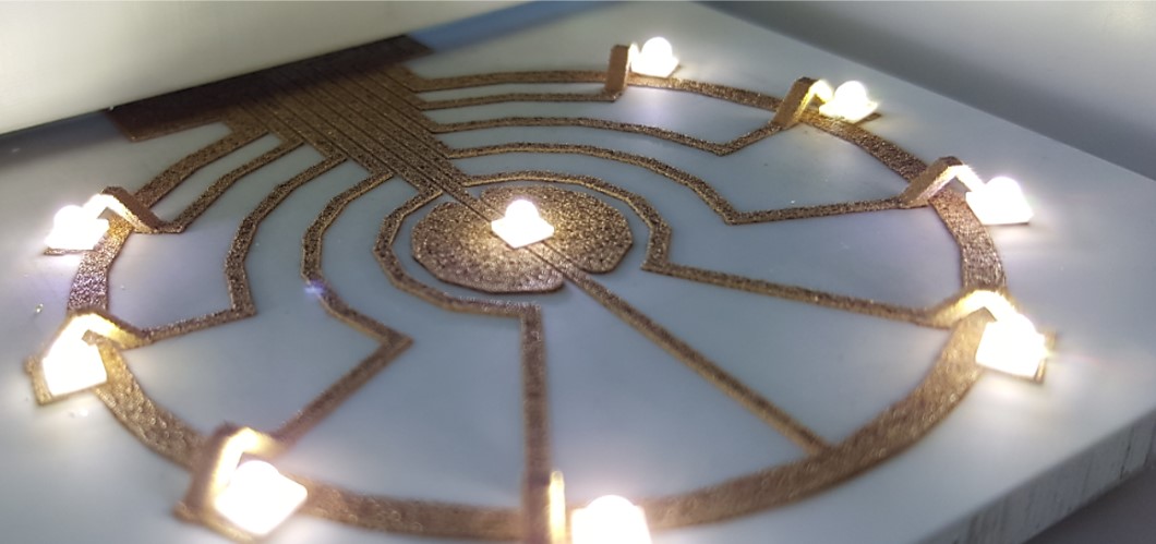
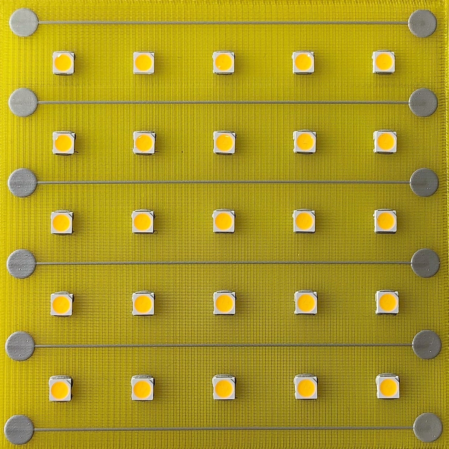
Additive manufacturing for the integration of resistive sensor technology in mechatronic systems – PreSens
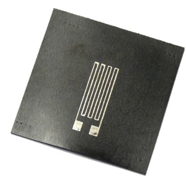
Although they rarely catch the eye, resistive sensors, which convert a mechanical load into an electrically measurable signal, have become indispensable in industry. They are used in weighing technology, in stress analysis, for example in structures such as bridges, or for torque measurement in machines. Another area of application is temperature measurement. The sensor is available as a finished component that just has to be integrated into the system to be monitored. Common designs are semiconductor-based sensors with high sensitivity for low loads or metal-based resistance sensors produced by etching and applied to foils. Disadvantages of the existing technology are a limited design freedom on 3D geometries and the typically required application of the sensors into the system in an additional assembly step.
The aim of the PreSens research project is to overcome these limitations by using digital printing technologies for sensor manufacturing, such as aerosoljet, piezojet and inkjet printing. On the one hand, the printing technologies enable the direct application of sensors to different carrier substrates and components. On the other hand, the sensors can be applied directly to 3D geometries in multi-axis printing systems, as will be used in the project, making it possible to image even complex sensor geometries.
In order to qualify the feasibility and suitability of digital printing for the production of resistive sensors, comprehensive printing tests will be carried out for this purpose and various media and substrate material systems will be researched. The manufactured sensors will be measured with respect to their sensor properties, such as accuracy, reliability and reproducibility, in order to determine suitable sensor principles. Strain gauges and temperature sensors will be investigated as sensors, which should be available in meaningful technology demonstrators by the end of the project.
The IGF project 09739 of the Research Association Räumliche elektronische Baugruppen is funded by the German Federal Ministry of Economic Affairs and Climate Action (BMWK) via the AiF within the framework of the program for the promotion of joint industrial research (IGF) on the basis of a resolution of the German Bundestag. The project is being carried out in collaboration with the Laboratory for Packaging and Interconnection Technology at Nuremberg Technical University. The project is accompanied by an extensive industry committee consisting of 14 companies with material and equipment manufacturers, as well as users.
Technology and Competence Center for the Characterization and Analysis of Power Electronic Systems – Laboratory for Characterization & Analysis of Power Electronic Applications – “Powerlyze-Lab”.
If we want to successfully advance the energy transition, one component is indispensable in the area of energy generation and use: power electronics. Regardless of whether energy is generated by photovoltaic or wind turbines or used in e-cars, e-scooters and pedelecs, or even at home in heat pumps and washing machines: wherever electricity flows, reliable and efficient power electronics modules are required to vary the voltage, frequency and current. As a module, power electronics is the necessary link between the socket or charging station on the one hand and the battery and electric motor on the other.
One of the goals of the Powerlyze Lab at Friedrich-Alexander-University Erlangen-Nuremberg (FAU) is to exchange technological developments more quickly between the university and cooperation partners from industry and business. In the technology and competence center of the Institute for Automation and Production Systems (FAPS), power electronic modules are characterized and analyzed, for which the European Regional Development Fund (ERDF) is providing around 650,000 euros over a period of three years.
The companies are to be put in a position to adapt their manufacturing processes and products to the constantly increasing demands of the market and to produce globally competitive power modules at the Bavarian location.
The project results are available beyond the ERDF project to all other research institutions and industrial companies for implementation, so that they can jointly contribute to achieving the agreed climate targets and mastering the energy transition. Herr Dipl.-Wirtsch.-Ing. Martin Müller will be happy to provide you with further information.