Project description
Molded interconnect devices (MIDs) are usually thermoplastic 3D substrate materials that are typically first laser direct structured (LDS) and then metallized with copper, nickel and gold without external current. In this process, the copper directly on the substrate acts as an electrical conductor, while the nickel layer provides the diffusion barrier to the gold surface. The latter enables various assembly and interconnection (AVT) techniques for electronic components, such as soldering, conductive bonding and wire bonding, to eventually obtain complex circuit carriers with a high integration density.
The reliability of metallic traces on LDS-enabled substrate materials is an essential prerequisite for the cross-breed application of MIDs. A survey of industry representatives on the subject of MID reliability revealed that delamination as well as the formation of microcracks in the conductive paths are the most common causes of MID failure. Efforts are therefore being made to eliminate these two causes as far as possible in order to significantly increase the reliability and service life of MIDs and to further promote their market penetration.
Challenge
Failure cause 1: Delamination
The choice of substrate material and the laser parameters used significantly influence both the bond strength between substrate and copper and the difference in their coefficients of thermal expansion. The latter is not only relevant for the application of MIDs at elevated temperatures, but also plays an essential role for AVT, e.g. during soldering.
Failure cause 2: microcracks
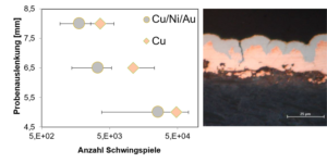
Studies within the scope of the AiF projects LDS-MID-ChaMP (16737N) and MetaZu (19754N) have shown that conductor cracks predominantly develop in the nickel layer. These microcracks expand by further loading and penetrate into the copper layer. If the load is too great, these eventually lead to failure of the conductive path and thus to failure of the circuit carrier.
Solution approach
In order to eliminate the two causes of failure mentioned above, the planned AiF project NiMm3 addresses three topics that build on each other.
1. interaction between substrate material and copper metallization
Various substrate materials are considered. In addition to thermoplastics, thermosets and ceramics are considered for an extended application range of 3D circuit carriers. By varying the laser parameter sets, the roughness and adhesion strength, and thus the reliability of the conductor track under mechanical and thermal stress (bending fatigue tests and environmental tests) are influenced. Imaging techniques such as ultrasonic microscopy (SAM) and the examination of transverse sections by scanning electron microscopy can provide further important insights.
2. alternative, nickel-free coating systems
Various nickel-free coating systems are investigated and compared with the established Cu/Ni/Au coating system. Possible variants are Cu/Ag, Cu/Sn, Cu/Pd/Au, Cu/Au and Cu/OSP (org. passivation). Here, too, conductive paths are examined under mechanical and thermal stress, among other things. Not only the layer system is varied, but also the layer thickness of the individual components.
3. AIT and influence of the soldering process
In MID technology, the assembly of electronic components is an essential step towards highly integrated circuit carriers. Therefore, the corrosion resistance and solderability or bondability of the different surface finishes are finally considered, as well as the influence of the soldering process on the adhesion strength of the metallization, e.g. by means of shear tests and SAM.

