Index
EffiBlech – CO2-effiziente elektrische Antriebe – Entwicklung einer industrietauglichen Prozesskette von gedruckten Magnetblechen (vom Pulver bis zum Bauteil)
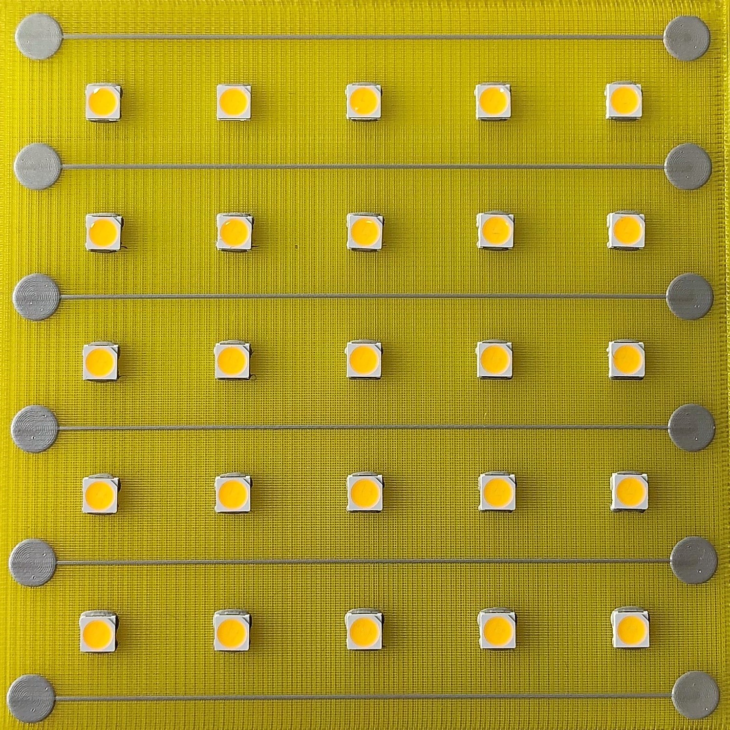
In elektrischen Antrieben entstehen bei der Energiewandlung Verluste, die zu einer Erwärmung der Maschine führen und abgeführt werden müssen. Zu den Gesamtverlusten tragen maßgeblich die Eisenverluste bei, die durch den Einsatz von Fe-Si-Elektroblechen reduziert werden können. Gängige Elektrobleche werden in aufwendigen mehrstufigen Umform- und Wärmebehandlungsprozessen hergestellt und anschließend zu Rotor- bzw. Statorblechpaketen verarbeitet. Bedingt durch die Prozessschritte Walzen und Stanzen ist die zu verarbeitende Minimaldicke der Bleche begrenzt und liegt standardmäßig zwischen 0,2 und 0,65 mm, weshalb eine weitere Reduzierung der Wirbelstromverluste nicht möglich ist. Weiterhin fallen bei der Formgebung der Elektroblechlamellen Materialverschnitte von bis zu 50 % an, so dass ein Großteil des unbenutzten teuren Materials erneut aufbereitet werden muss.
Das Forschungsprojekt EffiBlech wird im Rahmen des 7. Energieforschungsprogramms des Bundesministeriums für Wirtschaft und Energie (BMWi) gefördert und im Verbund mit industriellen sowie wissenschaftlichen Partnern durchgeführt. Der Lehrstuhl FAPS beteiligt sich in diesem Projekt in den kommenden drei Jahren mit der Erforschung von Produktions- und Prüfverfahren für eine pulvermetallurgisch-drucktechnische Herstellungsroute von dünnen Elektroblechen.
Die Firma Siemens fungiert als Projektkoordinator und ist sowohl bei der Erforschung der Pasten und des Druckprozesses als auch bei der Weiterverarbeitung und Prüfung der Bleche im Projekt beteiligt. Das Fraunhofer IFAM ist maßgeblich für die Pastenentwicklung und den Herstellungsprozess der Einzelbleche zuständig, wobei die Firma EKRA die Fertigungsanlage für den Druckprozess entwickelt. Ein wichtiger Verarbeitungsschritt ist die Wärmebehandlung der Bleche, weshalb sich die Firma MUT mit der produktspezifischen Entwicklung des Wärmebehandlungsprozesses im Rahmen des Projektes beschäftigt. Zur Gewährleistung der Bauteilqualität ist die Firma Optonic für die Integration geeigneter Inspektionssysteme zuständig. Die Arbeitspakete des Lehrstuhls FAPS fokussieren sich einerseits auf die Weiterverarbeitung der gedruckten Bleche und andererseits auf die Optimierung der Gesamtprozesskette. Ein Schwerpunkt liegt in der Erforschung potentieller Isolationssysteme sowie dessen Applikation, damit eine elektrische Trennung zwischen den Blechen sichergestellt wird und die Wirbelstromverluste minimiert werden. Weiterhin muss ein Konzept für die industrielle Einführung entwickelt und der Primärenergiebedarf des neuartigen Herstellungsprozesses analysiert und optimiert werden.
OptiWiRE – Optimierte Wickel- und Montageverfahren für recyclinggerechte Elektromotoren

Die Ziele des Vorhabens OptiWiRE, mit den Verbundpartnern ElringKlinger AG und dem Lehrstuhl FAPS, sind eine Verbesserung der Prozesskette bei der Herstellung von Elektromotoren, in Bezug auf der in der Automobilbranche sehr hohen Anforderungen an Taktzeit, Qualität und Flexibilität der Fertigung. Ein wesentliches Ziel, zu dem dieses Projekt beitragen soll, ist die Übergang von der Prototypen-Fertigung zur Vorserienproduktion. Weiter zielt das Vorhaben auf eine Effizienzsteigerung der Elektromotoren ab um eine höhere Lebensdauer der Motoren zu erreichen und um auch den Energieverbrauch von E-Fahrzeugen und die damit verbundene Reichweite zu erhöhen. Hinsichtlich der Leistungsfähigkeit kritische Fertigungsprozessschritten wurden bereits in Voruntersuchungen identifiziert. Dabei konnten wesentliche Optimierungspotentiale bei der Wicklungsherstellung am Stator und bei der Magnetmontage im Rotor festgestellt werden. Für diese beiden Prozessschritte sollen im Rahmen des Projektes Verbesserungen hinsichtlich des Produktes E-Maschine und der Produktion durch die Adaption neuer Verfahren erzielt werden.
Innerhalb des Gesamtvorhabens OptiWiRE wird im Teilvorhaben “füllgradoptimierte, automatisierte Statormontage von verteilten Einzugswicklungen” vom Lehrstuhl FAPS der FAU die Prozesskette der Statorproduktion ausgehend vom Statorblechpaket bis zur Kontaktierung der Stern- und Phasenverbinder betrachtet. Auf Grund von höheren Automatisierungspotentialen soll im Bereich der Stator-Fertigung das Einziehwickelverfahren für den industriellen Einsatz mit dem Ziel weiterentwickelt werden, flexibel auf Varianten- und Stückzahländerungen reagieren zu können. Ein wesentlicher Ansatz ist es dabei, den Draht definierter abzulegen, um den Kupferfüllgrad im Stator zu erhöhen sowie die Taktzeit des Prozesses zu verringern. Dies soll durch die flexible Automatisierung der dem Wickeln vor- und nachgelagerten Prozesse realisiert werden. So sollen insbesondere bei der Handhabung und Prozessführung von losen Leiterenden und Drahtbündeln deutliche Verbesserungen erreicht werden, um höchste Qualität und kürzeste Taktzeiten bei steigenden Produktionsmengen realisieren zu können.
Im Teilvorhaben “Prozessentwicklung beim Rotorbau – Fixierung der Magnete” untersucht die ElringKlinger AG die Optimierung der Rotorbaugruppe des im Projekt verwendeten Elektromotors. Das Verkleben der Magnete stellt den Stand der Technik im Bereich der Magnetmontage dar. Dies hat den Umgang mit Chemikalien, langen Prozesszeiten und aufwendigen Temperiervorgängen zur Folge. Durch die stoffschlüssige Verbindung von Magnet, Klebstoff und Rotorpaket lassen sich diese Komponenten nach der Lebensdauer des Motors im Recyclingprozess kaum noch voneinander trennen. Beim Versuch die Seltenen-Erde-Magnete aus dem Rotorpaket zu lösen zerbrechen diese. Eine sortenreine Trennung von Magneten und Blechmaterial ist ebenfalls durch die stoffschlüssige Verbindung des Klebstoffes erschwert. Rückstände des Klebstoffes bleiben an den Bauteilen haften. Diesen Herausforderungen stellt sich die ElringKlinger AG durch Entwicklungen von innovativen Magnetfixierungsstrategien.
Data based modelling of the selective wave soldering process to predict solder quality (SmartSelective)
ColEP – Collaborative Usage of Data in Electronics Production
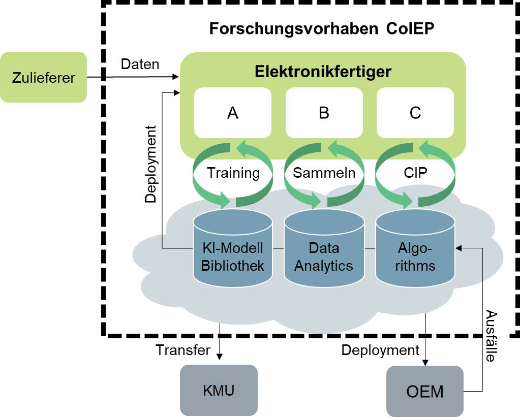
A key challenge for the use of data-based methods for the analysis and optimization of processes in electronics production is the imbalance of the data. Despite the large amounts of data generated in high-volume production, the information content of the data is limited, as the vast majority of inspections do not detect any errors. In order to avoid error slippage, the automated inspection steps, which are usually based on conventional image processing methods, are set so sensitively that there is usually a relatively high rate of pseudo errors. These components actually meet the specifications, but are incorrectly classified as faulty, resulting in a high manual inspection effort.
In order to reduce this effort, components identified as faulty can be rechecked using AI methods so that some of the pseudo faults are recognized, which results in a reduction of the testing effort. The quality of the AI methods used crucially depends on the amount and quality of the available data. In order to have a large database available despite the unbalanced data situation in electronics production, the research project ColEP is investigating the advantages and information technology solutions for the collaborative utilization of process, quality and metadata from electronics manufacturers and system manufacturers. Selected AI use cases in electronics production will be used to analyze potential improvements for which collaborative data sets appear particularly suitable. In this regard, the data is automatically anonymized and processed to ensure basic security. Furthermore, a framework will be developed using the GAIA-X concepts to ensure the sovereignty of the data for the owner.
In this context, both frameworks for federated learning and the integration into existing sovereign data infrastructures are examined. In contrast to centralized learning, where data from different sources is collected on a central server, federated learning keeps training data local to the participating companies at all times, ensuring data security and sovereignty. Model training takes place locally, after which the trained models are sent to a central server, which combines them into a global model.
The goal of the project is to investigate the applicability of federated learning in an industrial context using use cases in electronics production. It aims towards comparing the model performance of federated learning with centralized and local learning. In addition, data protection-specific advantages of federated learning will be investigated and security-relevant challenges such as data manipulation and reconstruction of training data will be critically examined and prevented using suitable methods.
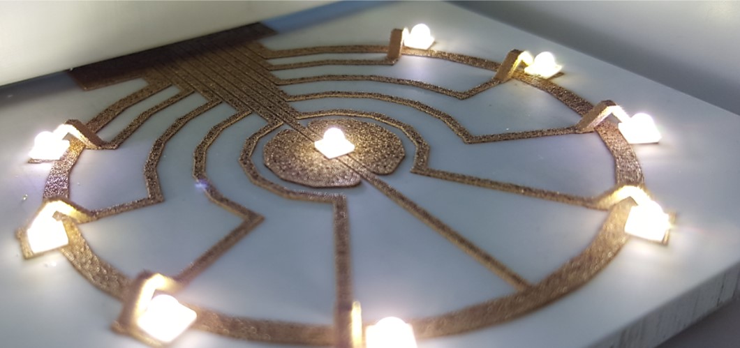
IntelRadar – Intelligent radar system through a combination of additive manufacturing, hardware-integrated computer architecture and smart test routines
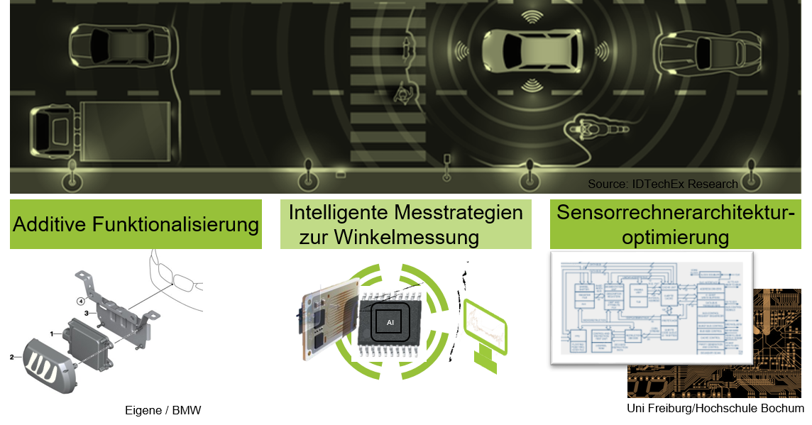
The desire for highly automated driving requires intelligent and networked vehicles that can detect their surroundings in detail and reliably using precise sensor technology. In addition to cameras, ultrasonic and lidar sensors, radar sensors are of great importance in the car of the future. Maximum accuracy and reliability, e.g. for radar-based environment detection at long distances of over 200 m, is essential. This is significantly influenced by signal scattering and attenuation, antenna quality and evaluation electronics, as well as algorithms. Due to these influences, the antenna, (secondary) radome (sensor cover) and evaluation electronics must be perfectly matched and integrated as a complete system as an essential prerequisite for precise detection. In order to minimize test and evaluation times, this also includes new approaches to functional testing through the use of artificial intelligence for sensor algorithms and sensor tests.
The aim of the project is to improve an automotive radar system along the production chain from the electronic architecture of the sensor, the development of an AI-supported test routine optimization of the angular calibration of the sensor and the integration of resistive radome heating elements by means of additive functionalization on free-form housings. This is intended to increase the reliability of the radar system. A holistic approach is being pursued, which is to be validated in the form of a demonstrator system at the end of the project.
Project goals
- Improvement of automotive radar systems
- Holistic view of the production chain
- Optimization of the radar hardware architecture
- Sensor test time reduction through AI algorithms
- Integration of resistive heating elements using printed electronics on 3D geometries
GoProMID – Genetically Optimized Product Design of Mechatronic Integrated Devices

Increasing digitalisation and the evolution of mechanical engineering products towards cyber-physical systems are driving the need for integrated functionalities. Innovative technologies such as Mechatronic Integrated Devices (MID) offer promising potential through the integration of mechanics and electrics/electronics, but result in a challenging development process due to the high product complexity. Product development requires complex and highly iterative manual optimizations and adjustments. Natural analogue principles show promising potential, but are currently mainly used in architecture, art or pure mechanical design. To realise the potential, a transfer is needed, including the development and integration of software-based support systems.
The GoProMID research project aims to develop the potential of biologically inspired methods and approaches in MID product development. The focus is on the use of generative design methods that allow the evolution of MID components based on a product specification – similar to the genetic coding of living organisms.For this purpose, established natural analogue approaches (e.g. genetic algorithms) are tested with regard to their suitability. In addition to the machine-usable formalisation of the design knowledge, the first software modules will be prototypically implemented and demonstrated in the context of meaningful use cases.
Additive Manufacture of Metal-Ceramic-Joints by means of Selective Laser Melting
Processes for additive manufacturing of 3D circuit carriers: Deriving design rules from reliability investigations
NiMm3 – Nickel-free metallization systems on 3D MID substrate materials
Molded interconnect devices (MIDs) are usually thermoplastic 3D substrate materials that are typically first laser direct structured (LDS) and then metallized with copper, nickel and gold without external current. In this process, the copper directly on the substrate acts as an electrical conductor, while the nickel layer provides the diffusion barrier to the gold surface. The latter enables various assembly and interconnection (AVT) techniques for electronic components, such as soldering, conductive bonding and wire bonding, to eventually obtain complex circuit carriers with a high integration density.
The reliability of metallic traces on LDS-enabled substrate materials is an essential prerequisite for the cross-breed application of MIDs. A survey of industry representatives on the subject of MID reliability revealed that delamination as well as the formation of microcracks in the conductive paths are the most common causes of MID failure. Efforts are therefore being made to eliminate these two causes as far as possible in order to significantly increase the reliability and service life of MIDs and to further promote their market penetration.
Challenge
Failure cause 1: Delamination
The choice of substrate material and the laser parameters used significantly influence both the bond strength between substrate and copper and the difference in their coefficients of thermal expansion. The latter is not only relevant for the application of MIDs at elevated temperatures, but also plays an essential role for AVT, e.g. during soldering.
Failure cause 2: microcracks
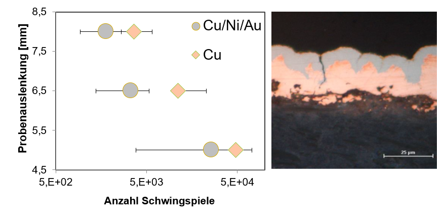
Studies within the scope of the AiF projects LDS-MID-ChaMP (16737N) and MetaZu (19754N) have shown that conductor cracks predominantly develop in the nickel layer. These microcracks expand by further loading and penetrate into the copper layer. If the load is too great, these eventually lead to failure of the conductive path and thus to failure of the circuit carrier.
Solution approach
In order to eliminate the two causes of failure mentioned above, the planned AiF project NiMm3 addresses three topics that build on each other.
1. interaction between substrate material and copper metallization
Various substrate materials are considered. In addition to thermoplastics, thermosets and ceramics are considered for an extended application range of 3D circuit carriers. By varying the laser parameter sets, the roughness and adhesion strength, and thus the reliability of the conductor track under mechanical and thermal stress (bending fatigue tests and environmental tests) are influenced. Imaging techniques such as ultrasonic microscopy (SAM) and the examination of transverse sections by scanning electron microscopy can provide further important insights.
2. alternative, nickel-free coating systems
Various nickel-free coating systems are investigated and compared with the established Cu/Ni/Au coating system. Possible variants are Cu/Ag, Cu/Sn, Cu/Pd/Au, Cu/Au and Cu/OSP (org. passivation). Here, too, conductive paths are examined under mechanical and thermal stress, among other things. Not only the layer system is varied, but also the layer thickness of the individual components.
3. AIT and influence of the soldering process
In MID technology, the assembly of electronic components is an essential step towards highly integrated circuit carriers. Therefore, the corrosion resistance and solderability or bondability of the different surface finishes are finally considered, as well as the influence of the soldering process on the adhesion strength of the metallization, e.g. by means of shear tests and SAM.
MultiPower – Customized production of highly-integrated electronic 3D power modules using multi-material vat photo-polymerisation, laser powder bed fusion and selective piezojet-metallization
The AiF-funded research project “MultiPower” aims at generating customized and highly-integrated electronic 3D power modules using various technologies of Additive Manufacturing. Multi-material photopolymerisation, laser powder-bed fusion and piezojet-printing are applied to create innovative designs with layerwise build-up. Thus, the development of suitable materials and stable processes is necessary as well as characterization and qualification of the produced interconnects. These works are accompanied and supported by simulation models.
Project advisory committee: ATN Automatisierungstechnik, Bach RC, Balver Zinn, Burms 3D Druck, Bosch Advanced Ceramics, Carbolite, GSB-Wahl, Heraeus Deutschland, Infinite-Flex, LOT-TEK, MetShape, Nanoscribe GmbH, Neotech AMT, Osram, Powerlyze, Rauschert Heinersdorf-Pressig GmbH, Rogers Germany, Schlenk AG, SEHO Systems, Sentinum, tangible engineering, Trainalytics GmbH, Vitesco, WIKA, Zollner.